


Overview
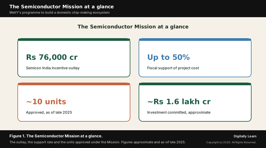
The India Semiconductor Mission, or ISM, is the Government's flagship programme to build a home-grown semiconductor and display manufacturing ecosystem. It is run by the Ministry of Electronics and Information Technology and sits inside the wider Semicon India programme, which carries a total incentive outlay of about Rs 76,000 crore. A semiconductor is the tiny chip that acts as the brain of every electronic device, from phones to cars to weapons. India has long imported almost all of its chips, so the Mission offers fiscal support of up to 50 per cent of project cost to firms that set up chip fabrication plants, packaging units and chip-design work in India. By late 2025 about ten projects worth roughly Rs 1.6 lakh crore had been approved, and ISM 2.0, announced in the Union Budget 2026-27, now widens the effort to equipment, materials and home-grown chip design.
What the India Semiconductor Mission Is: A Bid to Make Chips at Home
A Rs 76,000 crore Semicon India outlay run by MeitY
The India Semiconductor Mission, known as ISM, is the country's central effort to build a domestic semiconductor and display manufacturing ecosystem. It is the nodal agency that runs the broader Semicon India programme, which the Government approved with a total incentive outlay of about Rs 76,000 crore. The Mission was set up under the Union Cabinet's December 2021 decision.
ISM operates under the Ministry of Electronics and Information Technology, the MeitY, which is the nodal ministry for the whole effort. The Mission's purpose is plain: India has long imported almost all of its semiconductor chips, and the programme aims to bring chip design, fabrication and packaging onto Indian soil, so that the country makes more of this critical technology itself rather than buying it from abroad.
To do this, the Mission works mainly through money. It offers generous fiscal support, up to half the cost of a project, to companies willing to set up chip plants in India, and it pairs this with help on land, power, water and clearances from the states. By lowering the heavy upfront cost of a chip factory, the Mission tries to make India an attractive place to build one. The figure below sets out the Mission at a glance.
Why the Semiconductor Mission Is in the News: Units Cleared and ISM 2.0 Launched
From approval to approved units, and the launch of ISM 2.0
Why it matters now is that the Mission has moved from a scheme on paper to real factories taking shape. After the Semicon India approval, the Government began clearing individual chip units, so that public incentives are flowing into actual plants for assembly, testing and, for the first time, silicon fabrication in India.
The numbers are best read as approximate and as-of the Government's reporting, because more units are still being cleared. As of around late 2025, about ten semiconductor projects with a combined investment of roughly Rs 1.6 lakh crore had been approved across about six states. These include Micron's packaging plant and the Tata fab and packaging units, which are discussed in detail later in this briefing.
The second reason the Mission is in the news is ISM 2.0, announced in the Union Budget 2026-27. The first phase concentrated on attracting fabs and packaging plants; the new phase widens the aim to making semiconductor equipment and materials in India, designing full-stack Indian chip intellectual property, and strengthening the supply chains around the industry. Together, the new units and ISM 2.0 keep the programme firmly in the headlines.
Understanding the Significance of the Semiconductor Mission for India
Strategic autonomy, a smaller import bill and a high-tech ecosystem
What is the significance of the India Semiconductor Mission lies first in strategic autonomy. Chips are a critical technology that runs phones, cars, power grids, defence systems and artificial intelligence. The COVID-19 chip shortage and rising geopolitics showed how dangerous it is to depend on a handful of foreign suppliers, so making chips at home is a matter of national security, not just commerce.
Its second significance is economic. India spends heavily importing electronics and the chips inside them, and this large import bill drains foreign exchange. By building chip plants at home, the Mission seeks to cut that dependence, capture more of the value within India, and turn the country from a buyer of finished electronics into a maker of the components beneath them.
Its third significance is the ecosystem it can seed. A chip industry brings high-skilled jobs, draws global firms and their know-how, and supports the electronics, automobile, telecom and defence sectors that all need chips. In this way the Mission is a central pillar of Atmanirbhar Bharat, the drive for self-reliance, in one of the most strategic technologies of the age.
What Semiconductors Are: The Chip, and the Design-Fab-Packaging Value Chain
A material between conductor and insulator, and the brain of electronics
To follow the Mission, it helps to be clear on what a semiconductor actually is. A semiconductor is a material, most commonly silicon, whose ability to carry electric current sits between that of a conductor, such as copper, and an insulator, such as glass. This in-between behaviour can be controlled precisely, which is exactly what makes it useful for switching and processing electrical signals.
On a tiny sliver of such material, engineers build an integrated circuit, packing millions or billions of microscopic switches called transistors. This is the chip, and it is the brain of every electronic device. A modern phone, car, satellite or weapon system depends on chips to compute, store memory and control its functions, which is why chips are often called the new oil or the new strategic resource.
Because chips are so central, the country that designs and makes them holds real technological power. Making a leading chip is one of the hardest things in manufacturing, demanding extreme precision and very large investment. That difficulty is why only a few countries and firms dominate the industry today, and why India's effort to enter it through the Mission is so significant.
The value chain: design, fabrication and assembly-testing-packaging
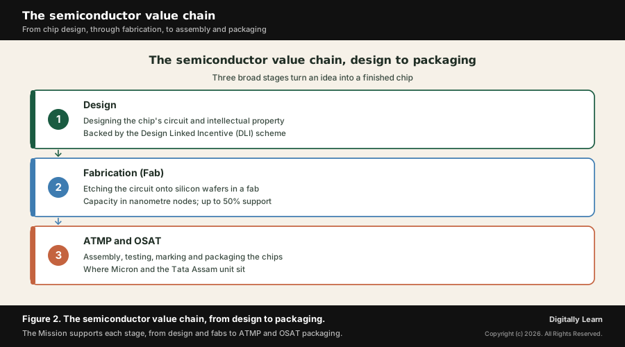
Making a chip runs through a long value chain with three broad stages. The first is design, where engineers lay out the chip's circuit and create the intellectual property behind it. India already has strength here, and the Mission's Design Linked Incentive scheme, the DLI, supports home-grown chip design to deepen it.
The second stage is fabrication, carried out in a plant called a fab. Here the designed circuit is etched onto silicon wafers through hundreds of precise steps. The fineness of a fab is measured in nanometre nodes: the smaller the node, the more advanced and powerful the chip. Fabs are extraordinarily costly, which is the main reason chip-making has stayed in so few hands worldwide.
The third stage is assembly, testing, marking and packaging, abbreviated as ATMP, also called outsourced semiconductor assembly and test, or OSAT. Here the finished wafers are cut, the chips are packaged into usable form, and each is tested. Most of India's first approved units, including Micron's plant, are at this packaging stage, which is a practical entry point into the industry. The figure below traces the chain.
How the Mission Works: Up to 50% Support for Fabs, Compound Units, ATMP and Design
Fiscal support of up to half the project cost
The engine of the Mission is fiscal support. Setting up a chip plant costs many thousands of crores, far more than most firms will risk alone, so the Government shares the burden. Under the scheme, the State offers support of up to 50 per cent of the project cost or capital expenditure, on a matching basis, to bring that upfront cost within reach.
This support is split across four routes, each aimed at a different part of the value chain. The first covers silicon semiconductor fabs, the plants that etch circuits onto wafers. The second covers display fabs, which make the screens used in phones, televisions and laptops, a related and equally import-heavy industry.
The third route covers compound-semiconductor and packaging units: compound-semiconductor, silicon-photonics and sensor fabs, along with ATMP and OSAT assembly-and-test plants. The fourth is the Design Linked Incentive scheme, which rewards Indian companies that design chips and build chip intellectual property. Together the four routes try to cover the whole chain, from design through fabrication to packaging.
| Support route under the Mission | What it covers | Fiscal support |
|---|---|---|
| Silicon semiconductor fabs | Plants that fabricate chips on silicon wafers | Up to 50% of project cost |
| Display fabs | Plants that make display screens | Up to 50% of project cost |
| Compound, ATMP and OSAT units | Compound-semiconductor fabs and assembly-test packaging plants | Up to 50% of capital expenditure |
| Design Linked Incentive (DLI) | Indian chip design and chip intellectual property | Up to 50% of eligible expenditure |
Read together, the four routes show the logic of the Mission: rather than back only the glamorous fabs, the State supports every link in the chain, so that India can enter where it is readiest, at packaging and design, while still attracting the harder fabrication plants. This is a deliberate use of public money to seed a whole new strategic industry.
The Approved Units and ISM 2.0: Micron, the Tata Fab, the Assam Plant and the Next Phase
Micron, the Tata Dholera fab and the Tata Assam packaging plant
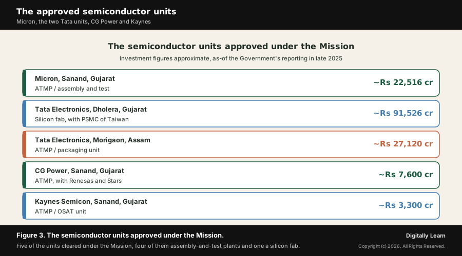
The first wave of approvals gave the Mission its flagship units. The earliest was Micron Technology's assembly-and-test plant at Sanand in Gujarat, cleared in 2023 with an investment of about Rs 22,516 crore. As a packaging unit, it was a practical first step, letting India enter the back end of chip-making while it built toward fabrication.
The most ambitious approval is Tata Electronics' silicon fab at Dholera in Gujarat, set up in technology partnership with PSMC of Taiwan, with an investment of about Rs 91,526 crore. This is India's first commercial chip fabrication plant, the hardest and most prized part of the chain. A second Tata Electronics unit, a packaging plant at Morigaon, also called Jagiroad, in Assam, was cleared at about Rs 27,120 crore.
Other approved units round out the picture. CG Power, with Renesas of Japan and Stars Microelectronics of Thailand, is building a packaging unit at Sanand at about Rs 7,600 crore, and Kaynes Semicon has a unit at Sanand at about Rs 3,300 crore. All of these figures are approximate and as-of the Government's reporting, since the count and totals keep changing as fresh units are cleared. The figure below lists the main units.
ISM 2.0: equipment, materials and full-stack Indian chip design
The Mission's next phase, ISM 2.0, was announced in the Union Budget 2026-27. Where the first phase concentrated on pulling in fabs and packaging plants, the second phase aims to deepen the ecosystem, so that India does not just assemble chips but commands more of the upstream technology behind them.
ISM 2.0 has three broad thrusts. The first is to make semiconductor equipment and materials in India, the specialised machines and chemicals a fab needs, which today come almost entirely from abroad. The second is to design full-stack Indian chip intellectual property, deepening the country's design strength into complete, home-owned chip designs.
The third thrust is to fortify supply chains and to set up industry-led research and training centres for technology and skills. A provision was made for the new phase in the Budget. In effect, ISM 2.0 marks a shift from simply building an ecosystem to consolidating it and integrating India more fully into the global chip industry.
The Benefits, the Real Challenges and the Global Subsidy Race
Jobs, capability and a foothold in a strategic industry
On the benefit side, a successful chip industry would be transformative. It would create large numbers of high-skilled jobs, from clean-room technicians to chip designers, and build deep engineering capability that spills over into the wider economy. It would also give India a foothold in an industry it has so far watched from the outside.
The gains are also strategic and economic. Domestic chips would shrink the electronics import bill, harden supply chains against shocks and sanctions, and secure the components that defence, telecom, automobiles and artificial intelligence increasingly depend on. For a Make in India economy aiming to move up the value chain, semiconductors are close to the top of the ladder.
Crucially, the Mission can also pull in private and foreign investment and the technology partnerships that come with it, as the Tata tie-up with PSMC and the CG Power link with Renesas show. Each plant builds suppliers, skills and confidence around it, so the benefit is not just one factory but the cluster that grows up alongside it.
Capital intensity, the technology gap, talent, water and power
A balanced view must weigh the challenges, the more so because UPSC questions reward this balance. The first is sheer capital intensity: a leading fab can cost tens of thousands of crores and must be replaced every few years as technology advances, so even a 50 per cent subsidy leaves a very large bill and a long, risky payback.
The second is the technology gap. The most advanced chips, made at the smallest nanometre nodes, are still produced abroad, and India depends heavily on foreign technology partners, equipment and talent to start. This is the heart of indigenisation of technology: India must absorb the know-how, then design and make the upstream equipment, materials and chip intellectual property itself. That is precisely the unfinished task ISM 2.0 targets, through home-grown equipment, materials and full-stack Indian designs.
Further hurdles are physical and structural, the logistics that decide whether a plant can run. A fab needs vast, uninterrupted supplies of clean power and water, world-class roads, ports and supply lines for its inputs, and long gestation periods before it earns a return. Ease of doing business helps at the margin, but it is these heavy logistics and infrastructure demands, not money alone, that ultimately decide whether the industry takes root.
Skill India and the Manufacturing Environment: Workforce, Labour and Factor-Market Reform
As the flagship Make in India effort in a critical sector, the Mission turns on more than incentives. A first condition is a deep pool of skilled people. Fabs, packaging plants and design houses run on specialised process engineers, materials scientists, clean-room technicians and chip designers, and India must build this talent at scale. This is the chip industry's Skill India test, and it is why ISM 2.0 adds industry-led research and training centres.
The second condition is a competitive manufacturing environment. Capital-intensive plants like fabs commit tens of thousands of crores for decades, so investors weigh the whole factor market before they build: reliable land, power and water, single-window clearances and predictable rules. Ease of doing business is therefore a precondition, since friction in approvals or factor supply can deter the very investment the subsidy is meant to attract.
Labour reform is part of that same factor-market story. Large manufacturing investment needs a stable, predictable framework for hiring, working conditions and industrial relations, and India has moved to simplify this by consolidating twenty-nine central labour laws into four Labour Codes. Even a capital-intensive fab still runs on a sizeable workforce, so clear, uniform labour rules, alongside skilling and ease of doing business, help make the Mission's long-horizon investments viable.
The global subsidy race and India's place in it
India's Mission unfolds inside a fierce global subsidy race. Worried by the COVID-19 chip shortage and by geopolitics, many governments are pouring public money into their own chip industries. The United States has its CHIPS Act, and the European Union, Japan, South Korea, Taiwan and China all run large incentive programmes of their own.
This race is a double-edged sword for India. On one hand, it confirms that semiconductors are a strategic priority worth subsidising, and it pushes global firms to diversify their plants beyond a few crowded locations, which India can court. On the other hand, it means India competes for the same investments, talent and equipment against far more experienced and deeper-pocketed rivals.
India's distinctive advantages are a large and growing home market, a strong base of chip-design engineers and political commitment at the highest level. Its task is to convert these into actual fabs and a real supplier ecosystem, moving steadily up from packaging and design toward advanced fabrication, without losing pace in a race where standing still means falling behind.
The Semiconductor Mission in Context: Atmanirbhar Bharat, Make in India and Digital Growth
How the Mission sits within India's self-reliance and digital push
Contemporary linkages place the Mission within India's larger drive for self-reliance. It is a flagship of Atmanirbhar Bharat and of Make in India in a critical technology, sitting alongside production-linked incentive schemes for electronics, mobile phones and other goods that together try to make India a manufacturing power, not only a services one.
The Mission also belongs to the story of India's digital growth. The same chips it seeks to make at home power the data centres, telecom networks, electric vehicles and artificial-intelligence systems that the economy is building rapidly, and policy efforts on AI and electronics now lean on a secure chip supply. In this sense semiconductors are the physical foundation beneath the digital economy.
Finally, the Mission is woven into India's strategic and diplomatic ties. Technology partnerships with the United States, Japan and Taiwan, and forums on critical and emerging technology, are part of how India secures the know-how and equipment a chip industry needs. It is one carefully funded piece of a much larger push for technological strength.
- Atmanirbhar Bharat and Make in India: The Mission is the flagship self-reliance effort in semiconductors, a critical and strategic technology.
- The PLI schemes: Production-linked incentives for electronics and mobiles complement the Mission in building a manufacturing base.
- The digital economy: Chips power data centres, telecom, electric vehicles and artificial intelligence, which all need a secure supply.
- Strategic technology diplomacy: Partnerships with the United States, Japan and Taiwan help India secure chip know-how and equipment.
Taken together, these linkages show that the Mission does not stand alone. It is the hardware end of a broader effort that runs from manufacturing incentives through digital infrastructure to technology diplomacy, all aimed at making India a maker, not merely a market, in advanced technology.
UPSC Relevance and Exam Focus
Where this fits in the UPSC-CSE syllabus
This topic maps most directly to General Studies Paper III: developments in science and technology and indigenisation of technology, and to the Indian economy, mobilisation of resources and the growth of the manufacturing sector. It also touches internal and external security, because chips are a strategic technology, and it links to the Make in India and Atmanirbhar Bharat themes that recur across the paper.
For Prelims, hold the high-yield facts: the India Semiconductor Mission runs under the Ministry of Electronics and Information Technology, within the Semicon India programme of about Rs 76,000 crore, and offers fiscal support of up to 50 per cent; it backs silicon fabs, display fabs, compound and ATMP or OSAT units and chip design through the DLI scheme; and ISM 2.0 was announced in the Union Budget 2026-27 for equipment, materials and Indian chip design.
For Mains, the recurring framing is to assess the Mission as a case of indigenisation of technology: weigh India's real achievements, a first commercial fab, packaging units and a design base, against the technology gap at advanced nodes and the heavy logistics and capital a fab demands, and examine critically how far self-reliance is realistic. A strong answer treats semiconductors as both an economic and a national-security project.
Recurring linked concepts an aspirant should keep in working memory:
- Semiconductor and chip: A material such as silicon, midway between conductor and insulator, on which the integrated-circuit chip that runs electronics is built.
- Fab, ATMP and node: A fab fabricates chips on wafers, ATMP or OSAT assembles and packages them, and the nanometre node measures how advanced a chip is.
- Semicon India and the DLI scheme: The Rs 76,000 crore programme and its design-linked incentive that together fund the chip value chain.
- Atmanirbhar Bharat and Make in India: The self-reliance and manufacturing drive of which the Mission is a strategic-technology flagship.
A common Prelims trap is to confuse the agencies and schemes. The India Semiconductor Mission is the nodal body under MeitY within the Semicon India programme; the Design Linked Incentive is its scheme for chip design, distinct from the production-linked incentive schemes for electronics and mobiles.
A common Mains trap is to praise the Mission without testing it. Its exam value lies in a balanced judgment: the genuine gains in strategic autonomy, a smaller import bill and high-tech jobs, set honestly against the capital intensity, the technology and talent gap, the heavy power and water needs and the fierce global subsidy race.
Previous Year UPSC-CSE Questions By the end you will be able to draft model answers for the following UPSC questions. Each question carries a collapsible framework showing how to approach it in the exam.
- UPSC Mains 2015 GS-III“Success of ‘Make in India’ programme depends on the success of ‘Skill India’ programme and radical labour reforms.” Discuss with logical arguments.
How to structure the answer in the exam
Body (sub-themes to develop):
- Make in India in a critical sector: the Semiconductor Mission is the flagship Make-in-India effort in chips, backing silicon fabs, ATMP/OSAT packaging and the Design Linked Incentive design scheme, with the Tata Dholera fab as India's first commercial fab and the Mission named as a flagship of Atmanirbhar Bharat.
- Skill India and the workforce: fabs, packaging plants and design houses run on specialised process engineers, materials scientists, clean-room technicians and chip designers that India must build at scale, so a deep skilled-talent pool is decisive, which is why ISM 2.0 adds industry-led research and training centres.
- Radical labour and factor-market reform: capital-intensive manufacturing like fabs depends on a competitive factor market, reliable land, power and water, single-window clearances and predictable rules, with ease of doing business a precondition and labour reform part of the same story, India having consolidated twenty-nine central labour laws into four Labour Codes.
- The logical balance: incentives are necessary but not sufficient, so the Mission's success in chips, as Make in India more broadly, depends on Skill India supplying talent and on labour and factor-market reform making the investment environment viable.
Sources and Further Reading
- PIB: India Semiconductor Mission
- PIB: Semicon India programme
- PIB: Cabinet approves three more semiconductor units under ISM
- PIB: India Semiconductor Mission (overview)
- PIB: Budget 2026-27 announces the launch of India Semiconductor Mission (ISM) 2.0
- PIB: India Semiconductor Mission 2.0
- MeitY: Ministry of Electronics and Information Technology
- NITI Aayog: Future of India's Semiconductor Industry roadmap
- DPIIT: Make in India (MII)
- PIB: Government Makes the Four Labour Codes effective
- Ministry of Labour and Employment: Labour Codes
- World Bank: Global Value Chains in the Electronics industry
- Wikipedia: Semiconductor device fabrication
- Wikipedia: Semiconductor industry in India
Editorial Disclaimer
This briefing is for UPSC preparation. Verify the figures and scheme details against the official MeitY and PIB sources before relying on them.


