


Overview
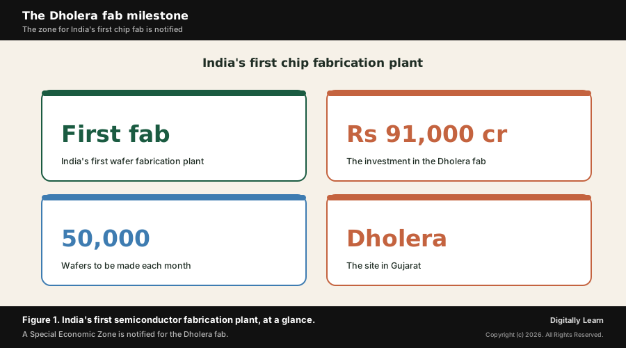
The Government of India has notified a Special Economic Zone at Dholera in Gujarat for the country's first semiconductor fabrication plant, a milestone reached in April 2026. The plant, a joint venture between Tata Electronics and Taiwan's Powerchip, will make silicon wafers, the hardest and most valuable stage of chip-making, with an investment of about 91,000 crore rupees and a planned capacity of 50,000 wafers a month. Unlike a packaging unit, which only finishes chips, a fabrication plant makes them from scratch, so the notification is an important step towards India producing chips on its own soil.
India Notifies the SEZ for Its First Semiconductor Fab
A regulatory milestone for the Dholera fabrication plant
The Government of India has notified a Special Economic Zone at Dholera in Gujarat for the country's first semiconductor fabrication plant, the milestone reached in April 2026. The zone, spread over about 66 hectares, is set up for Tata Semiconductor Manufacturing and is expected to provide work for around 21,000 people.
The plant is a joint venture between Tata Electronics and Taiwan's Powerchip, with an investment of about 91,000 crore rupees and a planned capacity of 50,000 silicon wafers a month. It is the most ambitious project so far under the country's drive to build a chip industry.
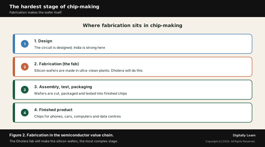
The key word is fabrication. Unlike a packaging plant, which finishes chips made elsewhere, a fabrication plant, or fab, makes the silicon wafers themselves in ultra-clean conditions. This is the hardest, most expensive stage, and India has never had one, which is why the Dholera fab is so significant.
Why a Domestic Fabrication Plant Matters
Fabrication is the hardest, most valuable stage of chip-making
Why it matters is that fabrication is the heart of the semiconductor industry. Making a wafer demands extreme precision, vast amounts of ultra-pure water and power, costly equipment and deep know-how, so the countries that can do it hold real technological power.
India has so far entered the chain only at the packaging end, where chips made abroad are finished into devices. A fabrication plant takes the country a stage deeper, towards making the chips themselves, and reduces the strategic dependence that comes from importing them.
The Significance of the SEZ Notification
Turning an approved project into a working enclave
What is the significance of this notification lies in turning a promise into a working site. The fab had already been approved and its foundation stone laid; notifying the Special Economic Zone gives it the legal status, duty benefits and single-window facilitation that a project of this scale needs to be built.
It is, however, a step on a long road, not the finish. Building and commissioning a fabrication plant takes years, and the real test will be whether the Dholera fab begins making working wafers at commercial scale. The notification is a serious move forward, but the chips themselves are still to come.
The Dholera Fab, the SEZ and the Value Chain
What the Dholera fabrication plant will do
The table sets out the key facts of the project, and the figure shows where fabrication sits in the chain that turns a design into a finished chip. The plant occupies the stage India has so far been missing.
| Feature | Detail |
|---|---|
| Partners | Tata Electronics and Powerchip (PSMC), Taiwan |
| Location | Dholera, Gujarat |
| Type of plant | A wafer fabrication plant, the first in India |
| Investment | About 91,000 crore rupees |
| Capacity | About 50,000 silicon wafers a month |
| Status | Special Economic Zone notified for the project |
The contrast with a packaging unit is the point to hold. A fabrication plant makes the wafers; an assembly, test and packaging unit only finishes them. The Dholera fab is the first to take on the harder, wafer-making job in India.
What a Special Economic Zone Is and Why a Fab Needs One
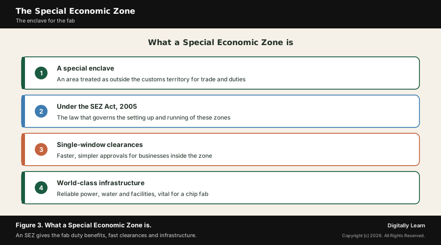
A Special Economic Zone is an area treated, for trade and duties, as if it were outside the country's normal customs territory. Governed by the Special Economic Zone Act of 2005, it lets businesses inside it import equipment and materials and export finished goods with duty and tax benefits.
For a chip fabrication plant, this matters a great deal. A fab imports vast quantities of specialised equipment, gases and materials, and the duty benefits, single-window clearances and reliable infrastructure of an SEZ make such a costly, complex project workable. Notifying the zone is therefore a practical enabling step.
What to Watch as the Fab Is Built
Three milestones on the road to home-made wafers
The notification points to three developments worth following, since a fabrication plant is built and ramped up over several years.
- (a) Construction and commissioning. Whether the Dholera fab is built and equipped on schedule and begins trial production of wafers.
- (b) The first home-made wafers. Whether the plant reaches commercial production, the moment India truly begins fabricating chips.
- (c) Ecosystem and water. Whether the supporting suppliers, trained engineers and the vast, reliable water and power supply a fab needs are secured.
The real test is whether the first fab moves from a notified zone and a foundation stone to a plant that reliably makes wafers, the stage that defines a genuine semiconductor industry.
Make in India, SEZs and Strategic Autonomy
How the fab connects to India's industrial strategy
Contemporary linkages tie the Dholera fab to the long effort to lift Indian manufacturing. It is a flagship of Make in India and of the India Semiconductor Mission, the government's nodal programme that offers large fiscal support to approved chip projects.
The use of a Special Economic Zone connects it to a familiar industrial-policy tool. SEZs, along with national investment and manufacturing zones and industrial corridors, are devices the state uses to concentrate world-class infrastructure and incentives in one place to attract large investment.
There are real challenges. A fab is one of the most demanding factories to build, needing huge volumes of ultra-pure water and uninterrupted power, a deep pool of specialised engineers and steady technology partnerships; sustaining the project to commercial output will test execution.
For India, the lesson is that the first fab is a long-term bet on strategic autonomy. Making chips at home, not just finishing them, is what would move the country from assembling electronics to truly manufacturing the components at their heart.
UPSC Relevance and Exam Focus
Where this fits in the UPSC-CSE syllabus
This topic maps to General Studies Paper III: the Indian economy, manufacturing and infrastructure, and developments in science and technology, with links to Make in India and indigenisation of critical technologies.
For Prelims, hold the key facts and distinctions: a fabrication plant, or fab, makes the silicon wafers, while a packaging unit only finishes chips; the Dholera fab is India's first fabrication plant; a Special Economic Zone is governed by the SEZ Act of 2005; and the India Semiconductor Mission is the nodal programme.
For Mains, the recurring framings are how chip fabrication advances self-reliance and Make in India, and how policy tools such as Special Economic Zones are used to promote high-value manufacturing.
Recurring linked concepts an aspirant should keep in working memory:
- Special Economic Zone: an enclave with duty and tax benefits, governed by the SEZ Act, 2005.
- Fabrication versus packaging: making the wafer versus finishing it into a usable chip.
- India Semiconductor Mission: the nodal programme that supports approved chip projects.
- Capital-intensive manufacturing: industries such as chip fabs that need huge investment rather than large labour forces.
A common Prelims trap is to think an SEZ promotes the export of services only. The SEZ Act aims at developing infrastructure and promoting investment and the export of both goods and services.
A common Mains trap is to call the notification the arrival of home-made chips. It is an enabling step; the fab must still be built and reach commercial production of wafers.
Previous Year UPSC-CSE Questions By the end you will be able to draft model answers for the following UPSC questions. Each question carries a collapsible framework showing how to approach it in the exam.
- UPSC Prelims 2010 GS-IThe SEZ Act, 2005 which came into effect in February 2006 has certain objectives. In this context, consider the following :
- Development of infrastructure facilities.
- Promotion of investment from foreign sources.
- Promotion of exports of services only.
Which of the above are the objectives of this Act ?
How to approach this Prelims question
Approach: Test each objective against the purpose of the SEZ Act.
Trap to watch: Statement 3 is wrong: the Act promotes the export of goods and services, not services only.
Key facts to recall:
- The SEZ Act, 2005 aims to develop infrastructure and promote investment, including from foreign sources.
- It promotes the export of both goods and services, not services alone.
Answer signal: Objectives 1 and 2 are correct; statement 3 is wrong, so the answer is 1 and 2 only.
- UPSC Prelims 2016 GS-IRecently, India's first 'National Investment and Manufacturing Zone' was proposed to be set up in
How to approach this Prelims question
Approach: Recall where India's first National Investment and Manufacturing Zone was proposed.
Trap to watch: It is a different instrument from an SEZ, though both are tools to promote manufacturing.
Key facts to recall:
- India's first National Investment and Manufacturing Zone was proposed in Andhra Pradesh (Prakasam district).
- Such zones, like SEZs, are policy tools to concentrate infrastructure and attract manufacturing investment.
Answer signal: The first National Investment and Manufacturing Zone was proposed in Andhra Pradesh.
- UPSC Mains 2017 GS-IIIAccount for the failure of manufacturing sector in achieving the goal of labour-intensive exports. Suggest measures for more labour-intensive rather than capital-intensive exports.
How to structure the answer in the exam
Introduction: Open with the goal of labour-intensive manufacturing for jobs and exports, and the reality of capital-intensive growth.
Body (sub-themes to develop):
- Causes: rigid labour rules, skill gaps and a policy tilt towards capital-intensive sectors such as chips and chemicals.
- Consequences: high-value output such as semiconductors creates fewer direct jobs per rupee invested.
- Measures: labour reforms, skilling, support for labour-intensive sectors such as textiles and leather.
- Balance: pursue high-value sectors such as semiconductors while not neglecting employment-rich industries.
Conclusion: Conclude that India must pursue capital-intensive frontiers such as chip-making while deliberately supporting labour-intensive exports for jobs.
Sources and Further Reading
- Press Information Bureau: Government notifies India's first chip fabrication plant at SEZ Dholera
- Press Information Bureau: India Semiconductor Mission, Tata Electronics and Tata Semiconductor Manufacturing sign fiscal support agreement for semiconductor fab
- Press Information Bureau: PM to lay the foundation stone of three semiconductor facilities
- Ministry of Electronics and Information Technology: Semiconductors and Display Fab Ecosystem
- Press Information Bureau: Cabinet approves semiconductor units under the India Semiconductor Mission
Editorial Disclaimer
This briefing is for UPSC preparation. Verify the latest project details against the official Press Information Bureau and Ministry of Electronics and Information Technology sources before relying on them.


