


Overview
India Semiconductor Mission, phase 2
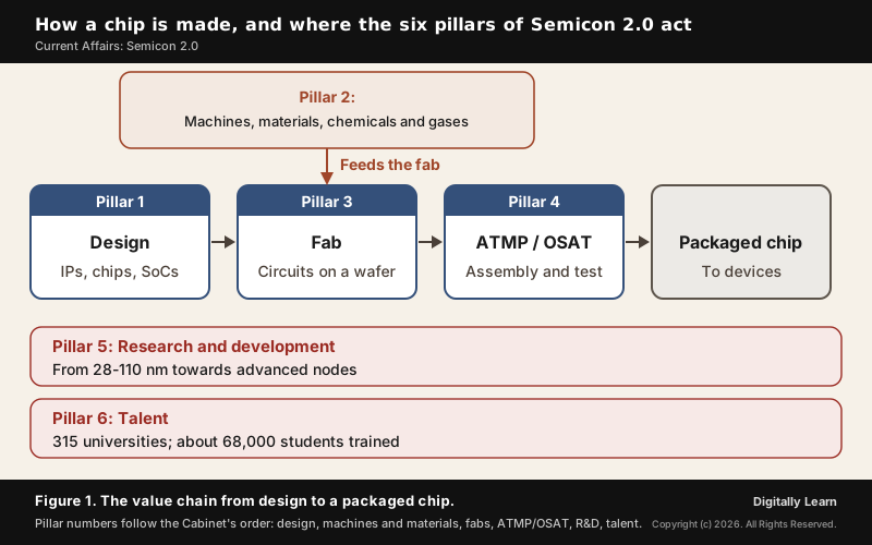
India Semiconductor Mission 2.0, approved by the Union Cabinet as Semicon 2.0 on 15 July 2026, is the second phase of India's programme to build a chip industry, with an outlay of Rs 1,27,500 crore over five years. It supports the whole chain, from chip design and the machines and materials of chipmaking to fabs, packaging, research and talent.
India Semiconductor Mission 2.0: The Cabinet Approval of July 2026
Semiconductor Mission 2.0: Outlay, Tenure and Targets
On 15 July 2026 the Union Cabinet, chaired by the Prime Minister, approved Semicon 2.0, the second phase of the India Semiconductor Mission, with a total budget outlay of Rs 1,27,500 crore. It builds on the first phase and is meant to give the semiconductor sector the sustained, long-term support that a chip industry needs.
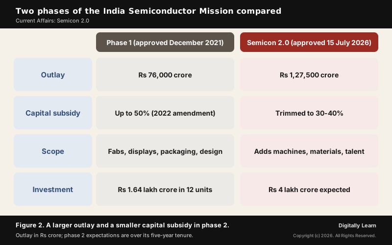
The approval came in steps. The Union Budget of 1 February 2026 announced ISM 2.0 to produce equipment and materials, design full-stack Indian IP and fortify supply chains, with industry-led research and training centres. On 1 July the Expenditure Finance Committee of the Finance Ministry cleared Rs 1.25 lakh crore, already well above the Rs 76,000 crore of the first phase, and on 15 July the Cabinet approved the final figure.
- Investment: About Rs 4 lakh crore expected to be drawn in.
- Production: Semiconductor output of about Rs 2 lakh crore.
- Exports: About Rs 1 lakh crore.
- Tenure: Five years; the details were then notified in the Gazette as the Scheme for development of Semiconductor Design and Manufacturing Ecosystem in India.
The same meeting approved Rs 62,500 crore for the Mobile Phone Manufacturing Scheme, which pays incentives of 2.25% to 5% on eligible sales depending on how much local design goes into a handset, because most components of phones assembled in India are still imported and Indian-designed handsets are rare.
Semiconductor Manufacturing in India: How a Chip Is Made
Design, Fabrication and Packaging: The Semiconductor Value Chain
A chip, or integrated circuit, is built in three broad stages. It is first designed; the design is then made on a wafer of pure single-crystal semiconducting material, almost always silicon, through many steps of photolithography, deposition, ion implantation and etching; finally the individual dies are cut from the wafer, assembled, tested and packaged.
- Chip design: Engineers create the circuit and its building blocks (intellectual property, or IP), using Electronic Design Automation software.
- Fabrication: A fab, or foundry, is the factory where integrated circuits are made; all fabrication happens inside cleanrooms where even a single speck of dust can ruin a microcircuit.
- Assembly and packaging: Units known as ATMP (assembly, test, marking and packaging) or OSAT (outsourced semiconductor assembly and test) turn dies into finished chips.
Companies that design chips but outsource making them are called fabless; foundries that make only others' designs are pure-play foundries. India's strength has been in design, while most of its approved factories so far are packaging units.
Semiconductor Fabrication Plant in India: Legacy and Frontier Nodes
A fab is among the costliest factories in the world: a new one costs over one billion US dollars and often tens of billions, and a single extreme ultraviolet (EUV) scanner can cost up to 340 million dollars. Each technology node, such as a 90 nm or a 28 nm process, names a generation of manufacturing.
Node names are given in nanometres, and a nanometre is one billionth of a metre (10-9 m). The figure in a node's name once gave the minimum feature size of the process; since 1994 it has become more of a marketing label with no fixed link to any physical dimension.
The most powerful phones use frontier chips of 7 nanometres or less. India's current facilities target 28 nm chips made on what are called legacy nodes, because everyday electronics, where size and computing power are not constraints, need such chips in large numbers. The first phase worked at 28 to 110 nm; Semicon 2.0 aims at more advanced nodes with research centres in India and abroad.
Semicon 2.0 Six Pillars: From Chip Design to Talent
The Six Pillars of Semicon 2.0
Semicon 2.0 is built on six pillars, so that the whole ecosystem grows rather than single factories.
- Design: With 105 startups already developing chips, the aim is to deepen the design ecosystem and develop IPs and designs of chips and systems, so that India becomes a key chip design IP country.
- Machines and materials: Firms that make and develop the machines, and the materials, chemicals and gases used in chipmaking, will be incentivised; this also builds precision manufacturing.
- More fabs: Silicon fabs, compound semiconductor fabs, discrete component fabs and display fabs, with the first fab scheduled for commissioning in 2028.
- ATMP and OSAT: More packaging units, with a focus on bringing in the most advanced packaging technologies.
- Research and development: From the 28 to 110 nm start towards advanced nodes and other advanced technologies, with leading R&D centres in India and abroad.
- Talent: 315 universities already train students in chip design on the latest EDA tools, and about 68,000 have been trained; training will deepen, and industry will help with cleanroom and fab construction skills.
The government says the scheme will support growth across sectors, strengthen national security through supply-chain resilience and help build technological leadership. The minister said the country would be self-reliant in producing indigenous chips by the end of the programme.
Design Pillar of Semicon 2.0: Strategic, Commercial and Deployment Support
The design pillar, the first of the six, has three categories of support, all limited to companies incorporated and headquartered in India with significant operations here.
| Category | What it supports | Key terms |
|---|---|---|
| 1. National importance | IP cores, chips, SoCs and modules for strategic priorities and critical infrastructure | Owned and controlled by Indian citizens; IP co-owned with C-DAC; projects preferably up to 6 years |
| 2. Commercial sector | Fabless chip design for commercial products | Seed funding of 50% of project cost or Rs 15 crore, whichever is lower; equity co-investment; royalty financing repaid at 5% of net revenue up to 1.5 times the support |
| 3. Deployment-Linked Incentive | New IP cores, chips and SoCs launched after the scheme | 9% of net sales for five years; up to Rs 30 crore per application and Rs 120 crore per company |
Design infrastructure comes with it: startups, MSMEs and academic institutions get central access to an EDA tools grid and to multi-project wafer fabrication, and design files and IP rights for commercial projects must remain in India.
What Changes from Phase 1: Wider Scope, Smaller Subsidy
The main change is scope. The Mission now covers a larger part of the electronics manufacturing ecosystem, including chip design talent, capital machinery, chemicals and gases of semiconductor-grade purity, and research, areas the first phase touched only partly. Even suppliers of raw materials, including minerals and gases, can be incentivised.
The money also works differently. A capital subsidy pays a share of a project's cost; phase 1 offered up to 50%, and Semicon 2.0 trims this to 30 to 40%, on the view that India is likely to become more attractive to chipmakers even with smaller incentives. Land support is also less likely, because States now offer land at token prices and their own incentives on top of the Centre's.
India Semiconductor Mission Phase 1: Twelve Units and Twenty-Four Designs
ISM 1.0: Approved Fabs, Packaging Units and Design Projects
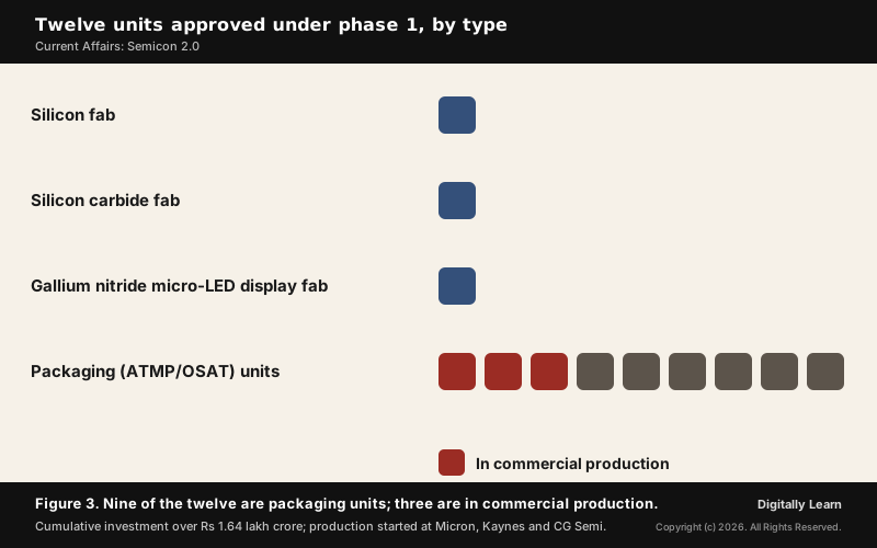
The first phase was approved in December 2021 with Rs 76,000 crore, and a 2022 amendment allowed capital subsidy of up to 50% for big projects such as Micron's memory chip packaging plant at Sanand, Gujarat. Twelve manufacturing units were approved, with cumulative investment of over Rs 1.64 lakh crore, to meet the chip needs of consumer appliances, industrial electronics, automobiles, power electronics, telecom and aerospace.
- Fabs: One silicon fab, one silicon carbide fab and an integrated gallium nitride micro-LED display fab.
- Packaging: Nine packaging units, spread across Gujarat, Uttar Pradesh, Punjab, Assam, Odisha and Andhra Pradesh.
- In production: Micron, Kaynes and CG Semi have started commercial production, and one more unit is expected to start in 2026.
Most of the investment has come from Tata Electronics. Its fab at Dholera, planned with Powerchip at a cost of Rs 91,000 crore, is to process 50,000 wafer starts a month on 28 nm technology and begin commercial production in 2028.
On the design side, 24 projects from startups and MSMEs have been approved for financial support under the design-linked incentive programme, and 105 startups and MSMEs have access to industry-standard design software. Their chips are for satellite communications, drones, surveillance cameras, Internet of Things devices, LED drivers, AI systems, telecom equipment and smart meters.
The government bought licences for costly design software and gives them free to universities and startups. The Semiconductor Laboratory at Mohali, being revamped, is to help "tape out" chips designed by students and researchers. Mohali has a long history in chipmaking: the state-owned facility there, run by Semiconductor Complex Limited, was crippled by a fire in February 1989, and production did not restart until 1997, which left India without domestic chip fabrication for years.
Semiconductor Industry in India: Strategic Rationale and Challenges
Supply-Chain Resilience and Strategic Leverage
From the supply-chain disruptions of the COVID-19 years to export controls in the trade war between the US and China, there has been a growing sense that India must fit more tightly into global electronics value chains. The world has also been short of memory chips, and chips are needed for artificial intelligence devices.
Chips carry strategic weight. A country that controls a scarce capability has leverage over others, and the best defence against supply shocks is to hold capabilities of one's own. The government holds that domestic capacity is essential even if it takes decades to reach countries such as the Netherlands and Taiwan.
Challenges for India's Chip Industry: Technology, Talent and Returns
- Frontier technology: Some tools are out of reach even for advanced economies; Dutch extreme ultraviolet lithography machines are so complex that only Japan is close to building one.
- Deep-pocketed rivals: Advanced economies spend far more to keep their place, and capabilities that give leverage invite resistance to India acquiring them quickly.
- Talent drain: India has many chip designers, but most work for foreign firms or on their behalf, so royalties and expertise stay abroad.
- Uncertain returns: Most phase-1 facilities have yet to begin commercial production, and the industry may not become a large employer.
The opportunity is real too. Semiconductor engineers and designers are sought worldwide amid a looming global talent shortage, and competing hard in key parts of the value chain could bring the kind of growth that made the Asian Tigers.
India Semiconductor Mission UPSC: GS Paper III Links
Industrial Policy and Technology in the GS Paper III Syllabus
Semicon 2.0 belongs to General Studies Paper III: industrial policy and its effects on industrial growth, indigenisation of technology, and science and technology developments. State PCS papers ask about the same economy and technology themes.
- Prelims facts: Approved 15 July 2026; outlay Rs 1,27,500 crore; five-year tenure; six pillars; capital subsidy 30 to 40% against up to 50% in phase 1; phase 1 approved December 2021 with Rs 76,000 crore; twelve units (one silicon fab, one silicon carbide fab, one GaN display fab, nine packaging units); 28 nm legacy node.
- Mains analysis: Why a country needs chipmaking, the design-to-packaging value chain, the shift from factory subsidies to ecosystem building, and the challenges of technology, talent and returns.
Previous Year UPSC-CSE Questions By the end you will be able to draft model answers for the following UPSC questions. Each question carries a collapsible framework showing how to approach it in the exam.
- UPSC Mains 2025 GS-IIIIndia aims to become a semiconductor manufacturing hub. What are the challenges faced by the semiconductor industry in India? Mention the salient features of the India Semiconductor Mission.
Answer outline: how to structure the answer
What the question asks, the main arguments, relevant examples and the direction of the conclusion. This is not a full model answer.
Introduction: Introduce semiconductors as the base of electronics and strategic security, and India's aim after COVID-era disruptions and export controls.
Body (sub-themes to develop):
- Challenges: fabs cost over a billion dollars; frontier tools such as EUV lithography are out of reach; rivals spend more; design talent works for foreign firms; most phase-1 units are not yet producing; the industry is not a large employer.
- ISM phase 1: approved December 2021, Rs 76,000 crore, capital subsidy up to 50%, twelve units (three fabs, nine packaging units) with Rs 1.64 lakh crore, 24 design projects, free EDA licences.
- Semicon 2.0: Rs 1,27,500 crore over five years; six pillars (design, machines and materials, fabs, ATMP/OSAT, R&D, talent); subsidy trimmed to 30-40%; targets of Rs 4 lakh crore investment and Rs 2 lakh crore production.
- Way ahead: deepen domestic IP and design, move from 28 nm legacy nodes towards advanced ones, keep talent at home.
Conclusion: Conclude that chipmaking is a decades-long effort in which steady policy and talent matter as much as subsidy.
Sources
- PMIndia: Cabinet approves Semicon 2.0 (15 July 2026)
- India Semiconductor Mission: Semicon 2.0, the six pillars and the design pillar
- Union Budget 2026-27: Budget Speech, paragraph 17 (1 February 2026)
- NCERT: Physics, Part I (Class XI), Appendices (units and prefixes)
- Wikipedia: Semiconductor industry in India
- Wikipedia: Semiconductor fabrication plant
- Wikipedia: Semiconductor device fabrication
- The Hindu, Delhi, 1 July 2026: FinMin panel clears Budget proposal of Rs 1.25 lakh crore for ISM 2.0
- The Hindu, Delhi, 16 July 2026: Cabinet okays Semicon 2.0, mobile, urea manufacturing schemes
- The Hindu, Delhi, 18 July 2026: Editorial, Promise of chips
- The Hindu, Delhi, 19 July 2026: What goals does Semicon 2.0 aim to achieve?
- UPSC: Civil Services Examination question papers
Editorial Disclaimer
This article draws on the Cabinet release, the India Semiconductor Mission and the other sources listed on this page.


